
Background
This is part of a larger project, to build a custom computer from discrete logic gates. There may be a series on that project in the future.
Like any modern(ish) computer, it should have a video card to display output to a monitor. The first successful video card was implemented using shared memory. This is enough for a POC (proof of concept), but its does not meet requirements for a production level product. Due to the memory being shared, the computer's need to write to the memory and the video card's need to display what is in the memory create timing conditions that either create a flickering effect or slow the frame rate.
To solve this problem, we need to have a way to let the computer update the memory regardless of when the video card needs to render pixels to the screen.
Double Buffer
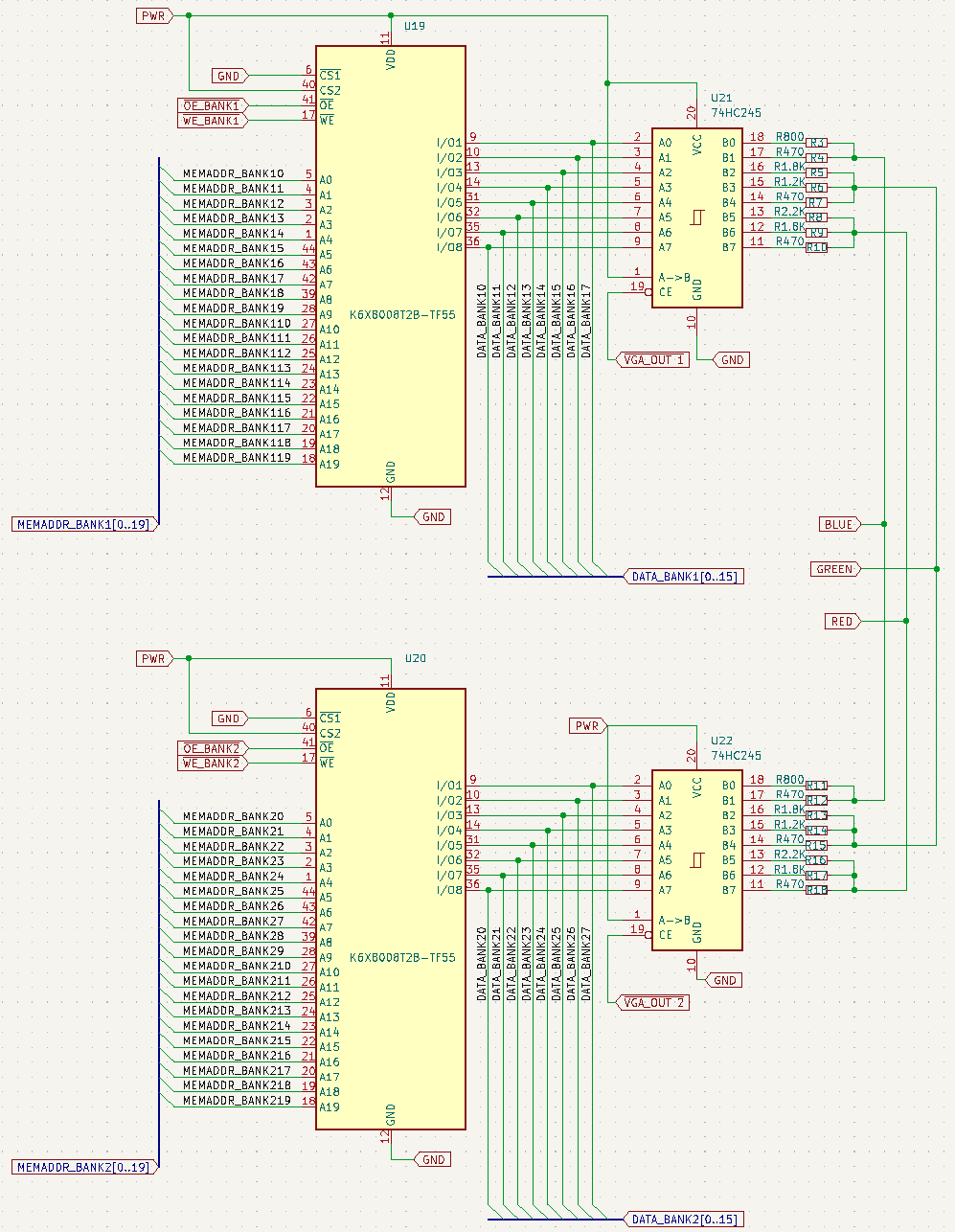
Enter double buffering. The concept is to use two separate memory banks. At any given time the video card is drawing from one bank, while the other is utilized by the computer to update what should be drawn next.
When the computer has finished updating the frame data, it sets a READY bit high, letting the video card know its time to swap.
The video card checks for this READY flag after each full screen draw. If its set, memory banks are swapped, and the video card can start to render from the newly updated memory bank, while the computer can safely write new data whenever there is a new frame that needs to be rendered.
Physical Design
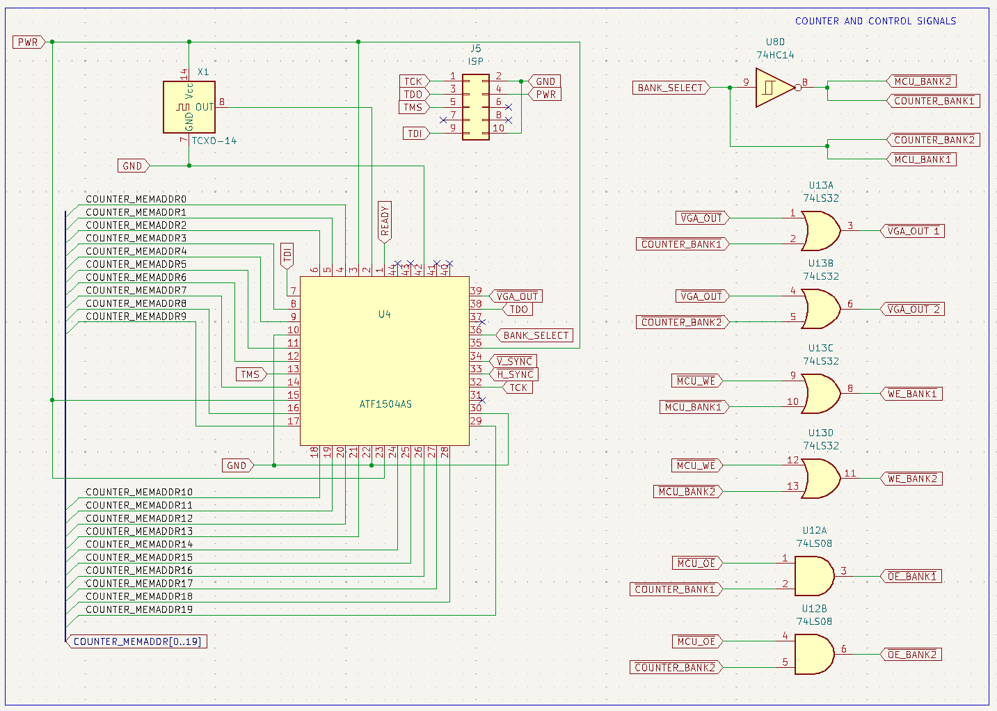
The predecessor video card relied on a set of ATF22V10C PLDs to process counter input. It's responsibility was to use combinational logic to determine H_SYNC and V_SYNC timing signals for VGA output.
The timing circuit relied on 74HC161 counters to generate x and y pixel counters. Unfortunately the timing of those chips is too slow for a 40MHz clock.
So in the new design, we have swapped in an ATF1504AS in place of the pair of old PLDs. The new PLD would also generate the counter signals on top of the predecessors responsibility to generate timing signals. It serves an additional critical purpose: generating the memory bank selection signal.
This did require redesigning the CUPL code.
The schematic has a few sections:
- Clock and CPLD for counter and timing signal generation, AND and OR gates for control signals
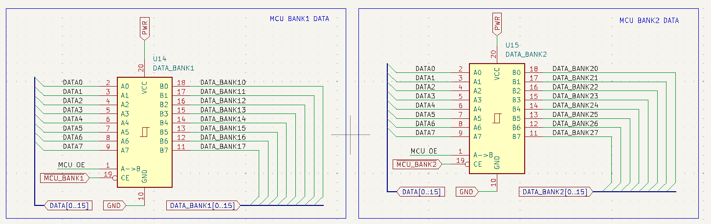
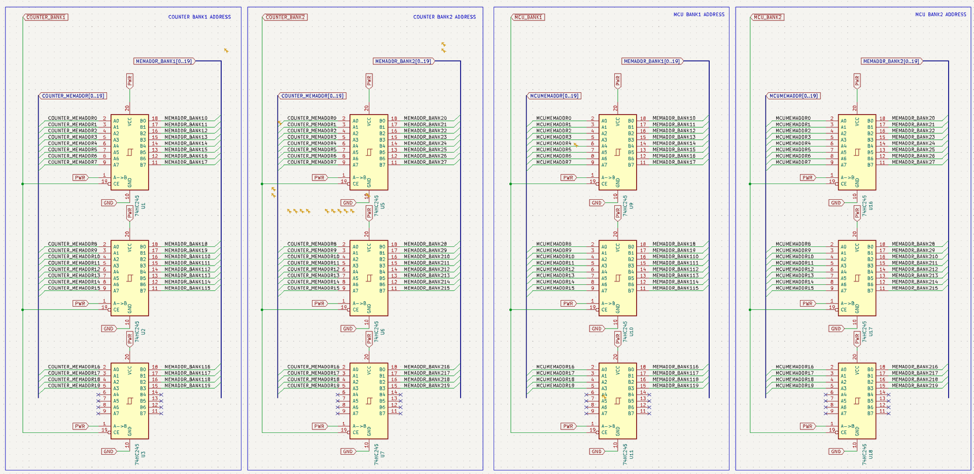
- Collections of gated bidirectional outputs for data and address controls
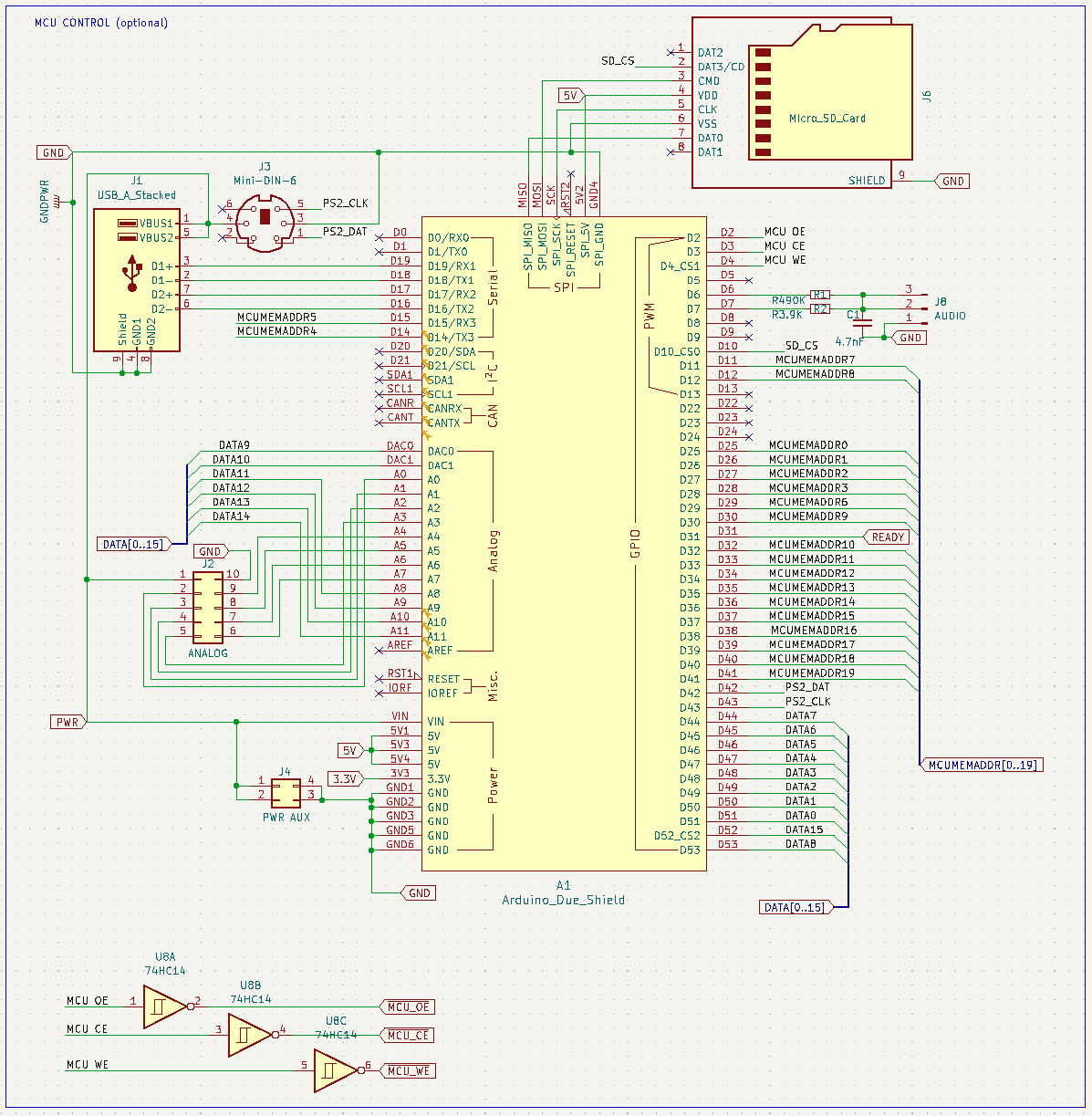
- MCU control
- Memory and gated video output
Then its just a matter of using our favorite KiCad software to layout a PCB
Electrical

3D rendering

What's Next?
Once the PCB is assembled, we will need to make changes to our Due VGA Library to adapt it to the new video card. More about that in a future entry.